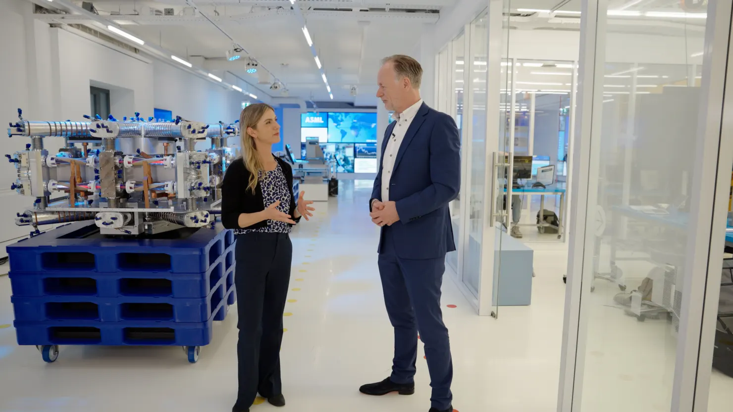
In a highly secure lab in the Netherlands, ASML has developed the world’s most advanced and expensive chipmaking machine—High NA, short for high numerical aperture. With a price tag exceeding $400 million, this massive machine is transforming semiconductor manufacturing. Developed over nearly a decade, High NA builds on ASML’s exclusive Extreme Ultraviolet (EUV) technology and represents a leap forward in resolution, efficiency, and performance. Measuring larger than a double-decker bus, the machine is composed of four major modules manufactured in the U.S., Germany, and the Netherlands, then assembled in Veldhoven for testing before being disassembled and shipped to customers.
Only five High NA systems have been shipped to date, with Intel’s Oregon fabrication plant receiving the first commercial installation in 2024. Customers like Intel, TSMC, and Samsung are using the system to manufacture the most advanced chips, with more companies like Micron, SK Hynix, and Rapidus expected to follow. High NA delivers significant improvements over previous EUV systems, including higher yield, faster production cycles, and the ability to project chip designs with greater precision using fewer steps. It enables chipmakers to etch smaller, more complex patterns onto silicon wafers with better efficiency, thanks to its larger lens opening that captures light at steeper angles.
The High NA machine retains the same EUV light source used in older systems, which relies on molten tin droplets being hit by lasers to create plasma hotter than the sun, emitting EUV light with a 13.5-nanometer wavelength. This light is absorbed by all known materials, necessitating a vacuum environment and specialized mirrors engineered by Zeiss, known for being the flattest in the world. Compared to the 193-nanometer wavelength used in ASML’s deep ultraviolet (DUV) machines, EUV—and especially High NA—enables projection of much finer features onto chips. The numerical aperture increase boosts resolution and reduces the need for multiple mask exposures, improving throughput and cost-efficiency.
Despite the high price, customers report strong returns on investment. Intel used High NA to produce 30,000 wafers and noted it is twice as reliable as earlier machines. Samsung observed a 60% reduction in cycle time, translating to chips that can complete more operations per second and lowering overall production costs. These gains are critical in the race to meet growing demands for AI, mobile, and computing hardware.
ASML has long held a monopoly in EUV lithography, with no viable competitor. While DUV systems are still part of its portfolio, accounting for 60% of its business in 2024, the future clearly lies in EUV and High NA systems. Due to export restrictions, China cannot access EUV machines, relying instead on DUV systems, which comprised nearly half of ASML’s sales in mid-2024. However, that percentage is expected to normalize.
To support growing U.S. demand, ASML is opening a major training center in Arizona and increasing shipments of High NA systems, with plans to produce 20 annually in the coming years. The company is also working on the next frontier—Hyper NA—expected by 2032 to 2035. With these advancements, ASML continues to shape the future of global chipmaking and maintain its leadership in one of the world’s most critical industries.
READ MORE: